by
by 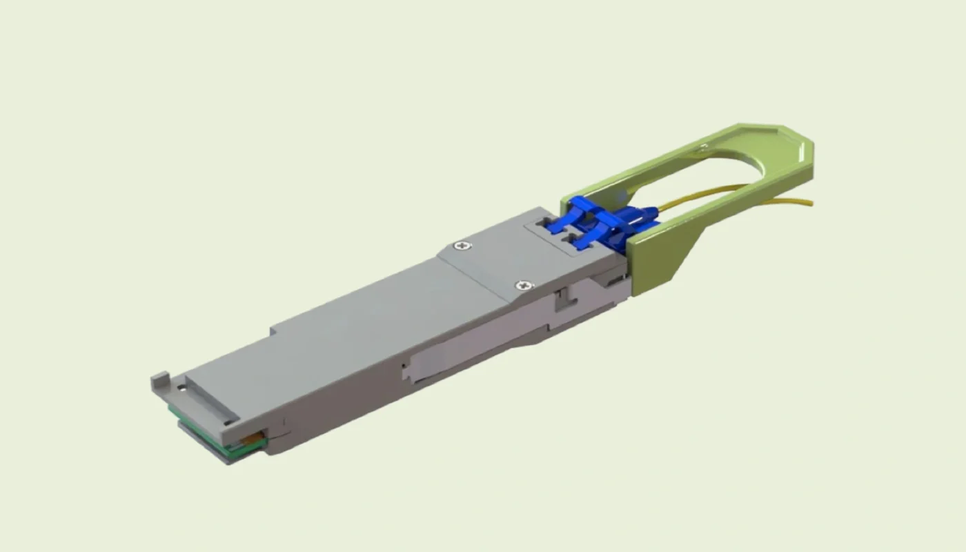
At present, the most prominent problems in electromagnetic compatibility testing of communication products are the electrostatic immunity and high-frequency electromagnetic radiation of optical modules. Optical module is one of the most important devices in communication, and its electrostatic protection is one of the prominent problems of electromagnetic compatibility of products.
Through specific electrostatic test cases, the reasons for the difference in the anti-static capability of the transceiver modules in the two optical modules due to different designs are analyzed, and the design measures for the electrostatic immunity of optical modules are proposed from the aspects of circuit design and structural design. The work done in this paper can provide reference and reference for the design, selection and EMC testing of optical modules.
This paper analyzes the difference in electrostatic immunity of two optical modules due to the different structural designs of transceiver modules through a test case of an SFP+ optical module and gives suggestions for improving the electrostatic immunity of optical modules from the aspects of circuit design and structure design. Disturbance design measures and recommendations.
The main electromagnetic interference sensitive points and electromagnetic interference radiation sources of the optical module are concentrated on the optical module circuit board, including key signals and key chips MCU, optical module and laser connection flex board or connecting wire, optical module electrical interface gold finger, TOSA, and ROSA . Except for the optical fiber interface area, the optical module is a fully enclosed structure. The optical modules TOSA and ROSA are the connection interfaces between the optical module and the optical fiber, so TOSA and ROSA are the main electromagnetic interference propagation channels of the optical module.
Page Contents
Electrostatic Interference Propagation Path of Optical Modules

Electrostatic discharge will generate a discharge current with a large amplitude and a short rising edge, and the discharge current will generate an electromagnetic field with a large intensity and a wide frequency. In particular, air discharge will cause multiple discharges, resulting in more serious electromagnetic interference.
From the theoretical analysis, it can be known that electrostatic discharge is a transient of voltage and current, and the radiated electromagnetic field, especially the near-field field, contains very rich frequency components. Using electric field probe, magnetic field probe and oscilloscope, the electromagnetic field generated by the discharge of the coupling plate of a certain brand of the electrostatic generator was measured. The test found that the electromagnetic field generated by ±6 kV discharge is mainly distributed in the frequency range of 20 MHz to 2 GHz, and the maximum radiation field is 104 dBμV.
Electrostatic discharge energy can enter electronic devices through direct conduction, capacitive coupling, and inductive coupling. When the circuit is close to the discharge point, the electric and magnetic fields around the circuit are very strong.
When the electrostatic gun conducts air discharge through the optical fiber metal reinforcing rib, there are also two interference modes: electromagnetic field interference generated by electrostatic discharge and conduction interference of electrostatic discharge current.
Electrostatic Immunity Design of Optical Module
Power Filtering
The transceiver circuit of the optical module needs to be isolated and designed, and the power supply of the transmitting end and the receiving end should be well-filtered. Generally, a π-shaped filter circuit is used to suppress the high-frequency electromagnetic interference coupled to the power supply. In order to make the filter circuit present as low impedance as possible in the interference frequency range caused by electrostatic discharge, three-stage capacitors are used in parallel, in which the 0.1 μF and 1 000 pF capacitors are placed as close as possible to the power pins of the chip, and the inductor and 10 μF capacitor can be placed away from the chip. The power pins are a little further away. Power ground traces on capacitors and inductors should be no less than 20 mil (about 0.5 mm) wide.
PCB Layout
During the PCB layout of the optical module, the key chips and the high-speed signal traces of the transceiver module should be placed in the center of the optical module circuit board as much as possible. The high-speed signal traces parallel to the gap between the metal shells of the optical module should be kept away from the edge of the circuit board as far as possible.
The stack-up design gives priority to ensuring that all high-speed signals (such as high-speed serial serdes signals) have a complete ground plane as a reference to meet the requirements of high-speed signal mirroring reflow. antenna. When the high-speed signal travels on the surface layer, it is necessary to perform ground wrapping processing on both sides of the high-speed signal. Ground holes are added to the copper edge of the ground wrapping, and the interval between ground holes is less than λ/20, which can reduce the crosstalk of adjacent signals. Strictly control the spacing between high-speed signal lines to ensure that the spacing meets the 3W (3 times the line width) principle.
Optical Module Design
For the metal casing of the transceiver module with poor shielding effect, a highly conductive elastomer gasket can be added between the metal casing of the optical module and the metal casing of the transceiver module to prevent oscillation in the optical module cavity.
The main reason for the case of the optical module electrostatic problem in this paper is that the packaging structure of the optical module transceiver components TOSA and ROSA is different. Therefore, if there is no special reason, the packaging structure of the transceiver module TOSA and ROSA should be made of metal materials, forming a metal material with the optical module housing.
Completely enclosed shielded cavity. If you must use plastic packages, you can paste absorbing materials on the TOSA and ROSA plastic packages, or stick absorbing materials on the flexible PCB boards or connecting pins where TOSA and ROSA are interconnected with the PCB, or on the disturbed sensitive chips. Paste the absorbing material on it.
Conclusion
The interference caused by static electricity to equipment can be divided into two types: conducted interference and radiated interference. For different equipment, specific analysis is required for different discharge forms, discharge voltages and discharge points. When solving the problem of electrostatic interference, different solutions should be taken according to the characteristics of the product itself.
All forms of EMC problems have three elements of EMC: interference source, propagation coupling path and receiver (interference source). This paper mainly analyzes and solves the electrostatic problem of optical modules from the perspective of propagation coupling path. If it is solved from the receiver aspect, it is to improve the anti-static interference ability of the optical module circuit, which is the next key research content. If starting from the interference source, it is to remove the interference source or reduce the interference intensity of the interference source.
The electrostatic problem in this paper is due to the air discharge of the fiber, so removing the interference source is to prevent the generation of the air discharge. A relatively simple method is to increase the thickness of the fiber insulation layer so that the air discharge of ±8 kV and ±15 kV cannot be generated.